 Download
Jedat Software “Amper” Certified on STARC’s Mixed-Signal Design Flow “STARCAD-AMS”
 Jedat Inc.
Jedat Software “Amper” Certified on STARC’s Mixed-Signal Design Flow “STARCAD-AMS”
2011.3.11
To Help STARC Members Ensure Advanced Mixed-Signal Chip Design
Chuo-ku, Tokyo, March 11, 2011 – Jedat, Inc. (headquarters: Chuo-ku, Tokyo, president & CEO: Shinichi Ishibashi, “Jedat”; Jasdaq: 3841) today announced that Semiconductor Technology and Academic Research Center (STARC)(headquarters: Shin Yokohama, Kohoku-ku, Yokohama, CEO: Katsuhiro Shimohigashi, “STARC”) has certified Amper, Jedat’s automatic placement tool for custom LSI, as the area estimation tool for STARC’s recommended mixed-signal design flow, STARCAD-AMS. Jedat Software “Amper” Certified on STARC’s Mixed-Signal Design Flow “STARCAD-AMS”In the evaluation of the functionality of high accuracy and high speed area estimation for analog blocks, STARC found that Amper was the only tool among several other competitive EDA tools, that sufficiently met STARC’s five criteria.
- 1. Observance of constraints
- 2. Pre-execution operation time of 5 or less minutes
- 3. Automatic placement in 5 or less minutes
- 4. Accurate placement result
- 5. Total placement time including manual correction when necessary
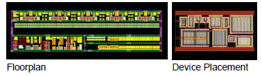
Amper is capable of estimating the area of analog blocks with high accuracy and at high speeds by observing the placement constraints (symmetry, pair, and alignment) registered in the circuit, and by utilizing its high accuracy device placement which takes into account the routing area. With this advanced ability, designers can obtain an extremely accurate floor plan result just as they had intended, in a very short time. Amper not only improves the efficiency of area estimation and floor plan but drastically reduces re-spins and significantly shortens the total design cycle. Amper can be used by plugging into Cadence’s design platform IC6.1.4(OA) as well as running on Jedat’s Alpha-SX design platform.
“In our evaluation, Jedat’s Amper was the only tool that has cleared our demanding targets, proving it is a very practical tool in the analog design field.” Said Mr. Kunihiko Tsuboi, general manager of the Mixed-Signal Development Group, 2nd Development Department at STARC. “Because a high accuracy area estimation result can be obtained quickly by using Amper, a review of the circuit design and specification, and examination of the trade-off with its size can be done at an early stage. This becomes an advantage for customer’s business, and critical re-spins can be prevented. Moreover, because a high accuracy floor plan can be done with short turn-around-time (TAT), re-spins from the layout design are reduced and high quality design can be realized. The final result is the shortening of the period of the entire post-layout verification.”
Custom LSI design including analog/mixed-signal is a critical portion of shortening the total design period of SoC design. Jedat’s goal is to shorten this design period to 1/10th of that when using existing flows. This can be achieved, Jedat believes, by offering a new solution into custom LSI markets while continuing the functional enhancement of a variety of design automation tools, including Amper.
About Amper
– Greatly reduces TAT of layout design through the setting of extensive constraint conditions and automatic device placement features –
Amper is an interactive high quality, high speed automatic device placer. Because it can estimate the routing area by processing the layout data as an abstract expression, it enables optimization while considering aspects of place & route. Devices such as MOS, BJT, resistors, and capacitors, can be placed. Block level and device group placement is possible with the tool. This capability can be applied to a wide variety of design fields, without regard to analog or digital circuit design. Extensive and strong constraint conditions can be automatically extracted in the layout editor, and interactively fixed if necessary. In addition, a high quality placement that considers detailed characteristic of devices can be achieved in a short time by running manual placement and automatic placement (partial placement function) alternately.
Benefits
- High quality and high speed automatic placement
- High quality placement while considering DC path
- Automatic optimal size determination by self adjustment features like number of device partitions
- Area optimization by automatic recognition of WELL electric potential
- Automatic placement while considering routing area
- High speed processing by a layout abstract expression
- Global routing feature enables placement while considering routing area
- Automatic mirror and rotation of placed devices
- Automatic packing capability of MOS transistors
- Partial placement
- Interactive execution in the layout editor
- Group placement
- Automatic extraction of constraint conditions
- Extensive constraint condition settings
- Automatic execution by change in device shape
- Outline placement specification
- Supports CMOS and BiCMOS process
About STARC
The Semiconductor Technology Academic Research Center, STARC, is a research consortium cofounded by leading Japanese semiconductor companies in December 1995. STARC’s mission is to contribute the growth of the Japanese semiconductor industry by developing leading-edge SoC design technologies. For more information, please visit http://www.starc.jp/index-e.html.
| Name | : | Semiconductor Technology Academic Research Center |
| Head Office | : | 17-2, Shin Yokohama 3-chome,Kohoku-ku,Yokohama 222-0033 Japan |
| President & CEO | : | Katsuhiro Shimohigashi |
| Capital | : | 440 million yen |
| Established | : | December 28, 1995 |
| Shareholders | : | Fujitsu Semiconductor Limited, Panasonic Corporation, Renesas Electronics Corporation, Rohm Co., Ltd., Sanyo Semiconductor Co., Ltd., Seiko Epson Corporation, Sharp Corporation, Sony Corporation, Toshiba Corporation |
About Jedat, Inc.
Jedat offers the custom LSI design environment “Alpha-SX series” that automates custom LSI design such as analog LSI, power device, LCD driver and memory. With the floorplan function (hierarchical operation, pin assignment, power supply and bus routing, etc.) and the automatic placement and routing tool for custom layout, Alpha-SX has brought significant improvement to the area where automation was previously difficult. Individual point tools are integrated in a constraint driven environment, and providing results via accumulation and reuse of design know-how. Distribution partners are located in Seoul (Korea), Beijing and Shanghai (China), Hsinchu (Taiwan) and the U.S. West Coast. These partners provide the same experienced customer support as Jedat offers in Japan. Visit Jedat on the web at www.jedat.co.jp.
| Headquarters | : | 3-4-14 Higashi-Nihonbashi, Chuo-ku, 103-00104, Tokyo |
| Operations began | : | February 2, 2004 |
| Capital | : | 760,007,110 Japanese yen |
| President & CEO | : | Ishibashi, Shinichi |
| URL | : | https://www.newjedat.arum-net.com/eng |
| Business descriptions | : | Research, development and sales of EDA software for designing IC (Integrated Circuit) and FPD (Flat Panel Display); related consulting services |
Click here for PDF version of the release.
